Growth and characterization of 2D materials using sputtering
ApplyProject Description
In this project, the student will be working on the growth of MoS2 using sputtering at different temperatures and characterizing them. The material will be later used in memory devices application.
 Division -
Computer, Electrical and Mathematical Sciences and Engineering
About the
Researcher
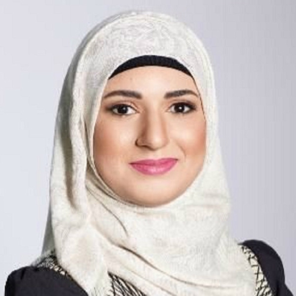
Nazek Elatab
Assistant Professor of Electrical and Computer Engineering

Professor El-Atab’s research focuses on the design and development of smart memory devices for in-memory sensing and in-memory computing applications. She is also interested in the design and development of advanced 3D/4D printed electronic devices for futuristic applications ranging from healthcare to agricultural and robotic applications, among others.
Desired Project Deliverables
Growth of MoS2 using sputtering at different temperatures
Characterization of the material - XRD, XPS, Raman, UV-Vis-NIR spectroscopy, AFM

